Introduction
Wafer Level Chip Scale Packaging (WLCSP) with electroless plating is an essential innovation in modern semiconductor fabrication, enabling miniaturized, high-performance integrated circuits suitable for the most demanding applications from mobile devices to automotive electronics. This technology not only helps in reducing package size and improving electrical and thermal performance but also simplifies assembly processes by applying uniform metal coatings at the wafer level before dicing.
According to Straits Research, “The global WLCSP electroless plating size was valued at USD 3,398.85 million in 2022. It is estimated to reach USD 5,596.93 million by 2031, growing at a CAGR of 5.7% during the forecast period (2023–2031).” This growth reflects increasing demand for advanced packaging that supports the miniaturization trend in semiconductors, driven by IoT, 5G, consumer electronics, and automotive sectors.
Understanding WLCSP Electroless Plating
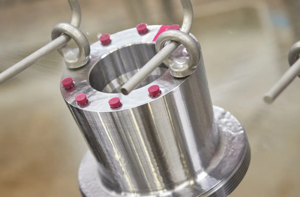
WLCSP involves packaging integrated circuits at the wafer level by redistributing pad layouts and attaching solder balls directly on the chip surface. Electroless plating, a core step in WLCSP, deposits thin, uniform layers of metals like nickel (Ni), gold (Au), or copper (Cu) on the wafer’s surface without the need for electrical power, ensuring excellent coverage of complex topographies.
This metal deposition technique is critical for forming Under Bump Metallization (UBM), which acts as an interfacial layer between solder bumps and the chip pads, enhancing adhesion, reducing oxidation, and improving electrical conductivity. Electroless plating provides superior control over film thickness and uniformity, essential for the reliability and performance of dense, small-pitch WLCSP packages.
Technological Trends and Innovations
Recent advancements in WLCSP electroless plating focus on improving process scalability, environmental sustainability, and integration with next-generation packaging:
-
Ni/Au Electroless Plating: Nickel provides a robust diffusion barrier, with an outer gold layer to prevent oxidation and facilitate solder wettability. Innovations target reducing gold thickness to cut cost while maintaining performance.
-
Environmentally Friendly Chemicals: New electroless plating baths are formulated to reduce toxic chemicals and wastewater, aligning with stricter environmental regulations in semiconductor fabrication.
-
Process Automation and Real-Time Monitoring: Automated wafer handling and inline metrology systems measure plating thickness and uniformity in real time, optimizing yields and throughput.
-
Integration with Fan-In and Fan-Out WLCSP: Electroless plating adapts across both fan-in WLCSP, where I/O pads remain within die area, and fan-out WLCSP, which redistributes pads over reconstituted wafers for higher I/O density.
-
Advanced Surface Preparation: Enhanced cleaning and activation techniques before plating increase adhesion and plating quality, crucial for smaller geometries and newer semiconductor materials.
Major Players and Competitive Landscape
Several companies worldwide lead efforts in WLCSP electroless plating technology, offering materials, equipment, or integrated processes:
-
Atotech (Germany): A major supplier of electroless plating chemicals and process solutions for semiconductor packaging, focused on sustainable and high-precision plating baths.
-
MacDermid Alpha Electronics Solutions (USA): Provides electroless Ni/Au plating chemistries tuned for advanced WLCSP and flip-chip applications.
-
Technic Inc. (USA): Specializes in plating solutions and surface finishing technologies used in WLCSP fabrication.
-
Sunjin Global (South Korea): A key provider of semiconductor plating equipment and process development services, particularly in advanced packaging domains.
-
Shin-Etsu Chemical (Japan): Supplies plating chemicals and related materials supporting wafer-level packaging processes in Asia.
-
Hitachi High-Technologies (Japan): Manufactures sophisticated plating and inspection systems with real-time metrology for process control.
-
Kokusai Electric (Japan): Develops plating tools and automation solutions emphasizing uniformity and minimal defects.
These companies compete on innovation, cost efficiency, and sustainability compliance, with geographic hubs spread across Asia, Europe, and North America.
Regional Updates and Market Dynamics
-
Asia-Pacific: The largest regional share is driven by Taiwan, South Korea, Japan, and China, home to leading semiconductor foundries adopting WLCSP electroless plating at scale. Investments in sustainable manufacturing and process automation are prominent.
-
North America: The US and Canada focus on innovation in plating chemistries and inline monitoring systems, supporting fab expansions for automotive and defense electronics.
-
Europe: Germany and Japan lead in high-precision plating solutions integrated with digital factory concepts, focusing on environmental sustainability.
-
Emerging Regions: India and Southeast Asia are ramping up packaging capacity, emphasizing cost-effective plating solutions to support growing semiconductor assembly sectors.
Recent Industry Developments
-
Atotech recently launched a novel electroless nickel plating bath with reduced phosphorus content, improving solder joint reliability and corrosion resistance in WLCSP structures.
-
MacDermid Alpha introduced automated plating process control software integrating AI-based defect detection, enabling higher throughput and yield improvements.
-
Hitachi High-Technologies unveiled next-generation wafer plating equipment featuring real-time thickness sensors, accelerating fab automation.
-
Several companies invested in R&D for electroless plating baths free from chromium and other hazardous materials, improving environmental compliance.
-
Collaborative projects between chemical suppliers and leading foundries aim at scaling fan-out WLCSPs with improved electroless plating process stability for higher I/O density packaging.
Challenges and Future Outlook
WLCSP electroless plating growth faces challenges like controlling plating uniformity for shrinking geometries, managing chemical waste sustainably, and scaling up for high-volume production at low cost. Maintaining plating adhesion on emerging substrate materials also requires continuous material innovations.
Despite these hurdles, the outlook remains positive, with expanding 5G, IoT, and automotive electronics demand driving adoption. Further integration of inline process monitoring, AI-based optimizations, and greener chemistries will enhance process reliability and sustainability.
The global WLCSP electroless plating sector is poised for steady growth, becoming a crucial technology enabling next-generation miniature, high-performance semiconductor packages worldwide.