The global semiconductor packaging market is entering a decisive growth phase, driven by rapid digitalization, rising semiconductor content per device, and the shift toward advanced integration technologies. The market is projected to grow from USD 49.89 billion in 2025 to USD 119.96 billion by 2034, expanding at a compound annual growth rate (CAGR) of 10.24% over the forecast period.
Semiconductor packaging plays a critical role in protecting integrated circuits while enabling electrical connectivity, thermal management, and mechanical stability. As semiconductor devices become smaller, more powerful, and more complex, packaging has evolved from a back-end process into a key differentiator for performance, efficiency, and system reliability.
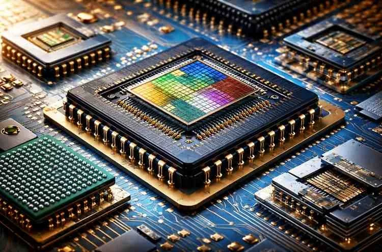
The increasing adoption of advanced packaging technologies such as flip-chip, fan-out wafer-level packaging, system-in-package, 2.5D, and 3D integration is redefining the competitive landscape. These technologies are essential to meet the performance requirements of 5G, artificial intelligence, high-performance computing, autonomous vehicles, and data centers.
Regionally, Asia Pacific dominated the global market with a 54% share in 2024, supported by its strong electronics manufacturing base and mature semiconductor ecosystem. At the same time, North America is emerging as the fastest-growing region, driven by large-scale government initiatives such as the U.S. CHIPS and Science Act, which is accelerating domestic semiconductor packaging R&D and manufacturing capacity.
Market Dynamics
Driver: Increasing Densification and Miniaturization
The ongoing trend toward smaller, lighter, and more powerful electronic devices is a primary driver of semiconductor packaging demand. Consumer electronics, wearables, IoT devices, and automotive electronics require high functionality within limited physical space. This has significantly increased the need for packaging materials capable of supporting high pin density, efficient heat dissipation, and signal integrity.
Advanced packaging solutions enable higher levels of integration while maintaining reliability under thermal and mechanical stress. Materials such as organic substrates, advanced polymers, encapsulation resins, and thermal interface materials are essential to meeting the stringent requirements of modern electronics.
Restraint: High Cost of Raw Materials and Skilled Workforce Shortage
The semiconductor packaging market faces challenges related to the high cost of advanced raw materials and manufacturing processes. Developing next-generation packaging solutions requires substantial R&D investment, specialized equipment, and skilled labor. These factors raise production costs and can slow adoption, particularly among smaller manufacturers.
Additionally, the shortage of trained packaging engineers limits scalability, especially for advanced and heterogeneous integration technologies.
Opportunity: Inorganic Growth and Strategic Collaborations
As demand rises for high-performance semiconductor solutions, leading players are increasingly adopting inorganic growth strategies, including partnerships, joint ventures, and co-investment models. These collaborations help accelerate innovation, expand production capacity, and reduce time-to-market.
A notable example is the US-JOINT initiative, launched in July 2024, bringing together Japanese and U.S. semiconductor materials and equipment companies to advance back-end process R&D through a shared research facility in the United States.
Frequently Asked Questions
What is driving the growth of the semiconductor packaging market
The market is driven by miniaturization, rising demand for high-performance chips, adoption of AI and 5G, and advancements in advanced packaging technologies.
Why does Asia Pacific dominate the semiconductor packaging market
Asia Pacific benefits from strong manufacturing ecosystems, cost efficiency, skilled labor, and high consumer electronics demand.
What role does advanced packaging play in semiconductor innovation
Advanced packaging enables higher performance, better power efficiency, and system integration without relying solely on smaller process nodes.
How does the U.S. CHIPS Act impact semiconductor packaging
The CHIPS Act provides funding to boost domestic packaging R&D, reduce reliance on Asia, and strengthen the U.S. semiconductor ecosystem.
Which end-use industry generates the highest demand for semiconductor packaging
Consumer electronics remains the largest end-use segment due to high semiconductor volumes in smartphones, wearables, and computing devices.
Source : https://www.towardspackaging.com/insights/semiconductor-packaging-market-sizing