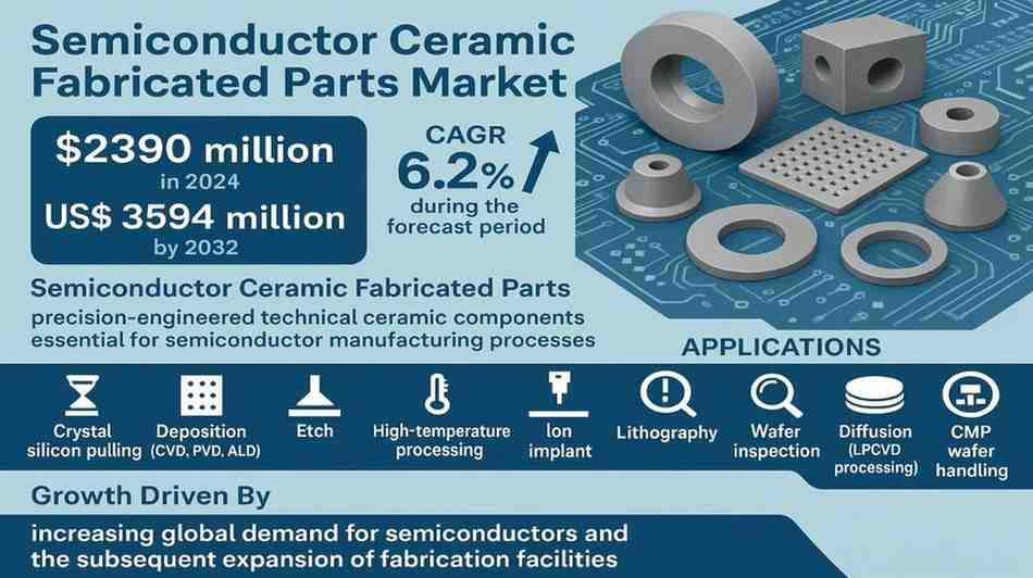
Semiconductor Ceramic Fabricated Parts Market, valued at USD 2390 million in 2024, is poised for substantial growth, projected to reach USD 3594 million by 2032. This expansion, driven by a compound annual growth rate (CAGR) of 6.2%, is detailed in a comprehensive new report published by Semiconductor Insight. The study underscores the indispensable role these precision-engineered components play in enabling advanced semiconductor manufacturing processes, where material purity, thermal stability, and mechanical integrity are non-negotiable.
Semiconductor ceramic fabricated parts, including components like electrostatic chucks, heaters, showerheads, and wafer handling arms, are fundamental to maintaining process control and yield in fabrication equipment. Their ability to withstand extreme temperatures, corrosive environments, and maintain ultra-high vacuum compatibility makes them critical for deposition, etch, lithography, and other key process steps. As chip geometries shrink below 5nm, the demand for components with tighter tolerances and enhanced material properties is accelerating, solidifying the strategic importance of this market.
Semiconductor Fabrication Expansion: The Core Growth Catalyst
The report identifies the unprecedented global investment in semiconductor manufacturing capacity as the primary driver for market growth. With the semiconductor application segment consuming over 90% of all fabricated ceramic parts, the correlation is direct and powerful. The semiconductor equipment market itself, a key consumer, is projected to sustain annual expenditures exceeding $100 billion, creating relentless demand for high-performance ceramic components.
"The concentration of leading-edge semiconductor fabs and equipment OEMs in the Asia-Pacific region, which accounts for nearly 75% of global ceramic part consumption, is the central nervous system of this market's momentum," the report explains. With announced global investments in new fabrication facilities surpassing $600 billion through the end of the decade, the need for reliable, high-purity ceramic solutions is intensifying. This is especially true for advanced EUV lithography and atomic-layer deposition processes, where part flatness must be maintained within sub-micron tolerances and thermal uniformity is critical.