https://www.relianceauh.ae/hangsterfers.html
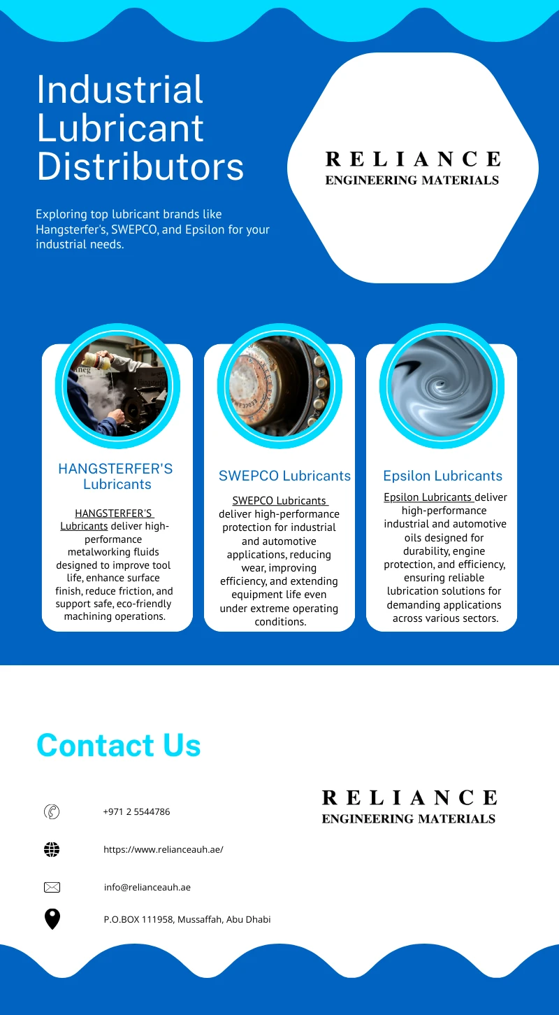
Reliance Engineering Materials is a trusted name in the UAE’s industrial sector, delivering high-quality engineering products and solutions across various industries. With a strong focus on performance, reliability, and customer satisfaction, we specialize in the supply and distribution of premium-grade lubricants and engineering consumables. As Industrial Lubricant Distributors, we offer a comprehensive range of high-performance products from globally recognized brands such as SWEPCO Lubricants and HANGSTERFER'S Lubricants. We are also a leading grease supplier in the UAE, providing specialized lubrication products that enhance machinery lifespan, reduce downtime, and improve operational efficiency.
Reliance Engineering Materials is a trusted name in the UAE’s industrial sector, delivering high-quality engineering products and solutions across various industries. With a strong focus on performance, reliability, and customer satisfaction, we specialize in the supply and distribution of premium-grade lubricants and engineering consumables. As Industrial Lubricant Distributors, we offer a comprehensive range of high-performance products from globally recognized brands such as SWEPCO Lubricants and HANGSTERFER'S Lubricants. We are also a leading grease supplier in the UAE, providing specialized lubrication products that enhance machinery lifespan, reduce downtime, and improve operational efficiency.
https://www.relianceauh.ae/hangsterfers.html Reliance Engineering Materials is a trusted name in the UAE’s industrial sector, delivering high-quality engineering products and solutions across various industries. With a strong focus on performance, reliability, and customer satisfaction, we specialize in the supply and distribution of premium-grade lubricants and engineering consumables. As Industrial Lubricant Distributors, we offer a comprehensive range of high-performance products from globally recognized brands such as SWEPCO Lubricants and HANGSTERFER'S Lubricants. We are also a leading grease supplier in the UAE, providing specialized lubrication products that enhance machinery lifespan, reduce downtime, and improve operational efficiency.
0 Comments 0 Shares